
A power supply circuit board is the beating heart of every electronic device. Whether it's a smartphone charger, an industrial motor controller, or a mission-critical defence system, the power supply PCB is responsible for converting raw incoming AC mains power — or a DC battery source — into precisely regulated, stable DC voltages that every component on the board depends on. Without a well-designed power supply section, even the most sophisticated microprocessor or FPGA is rendered useless.
In this in-depth guide, the AEAR PCB Design Team walks you through every critical aspect of power supply circuit board design — from fundamental component selection to advanced layout techniques and mandatory safety protocols. Whether you are a seasoned hardware engineer or a procurement manager evaluating PCB suppliers, this article equips you with the technical knowledge to make informed decisions.
1. Introduction to Power Supply Circuit Boards
At its core, a power supply circuit board — often abbreviated as PSU PCB — is a dedicated section of a printed circuit board (or a standalone board) that conditions electrical power for the rest of the system. The primary function is to convert the available input power source into one or more regulated output voltages that meet the specific requirements of downstream circuits.
The input can be alternating current (AC) from a wall outlet — typically 110V/230V at 50/60 Hz — or direct current (DC) from a battery, solar panel, or vehicle electrical system. The output is almost always DC, commonly at voltages like 3.3V, 5V, 12V, 24V, or ±15V, depending on the application.
Key Insight
Approximately 30-40% of field failures in electronic products can be traced back to power supply issues — making PSU PCB design arguably the most critical discipline in electronics engineering. A robust power supply design is not an optional add-on; it is the foundation of product reliability.
Modern power supply PCBs must balance competing requirements: high efficiency to minimize heat and energy waste, tight voltage regulation for sensitive digital logic, low electromagnetic interference (EMI) to meet regulatory standards, compact form factors for portable devices, and — above all — absolute safety for both the end user and the equipment itself.
2. Core Components of a Power Supply PCB
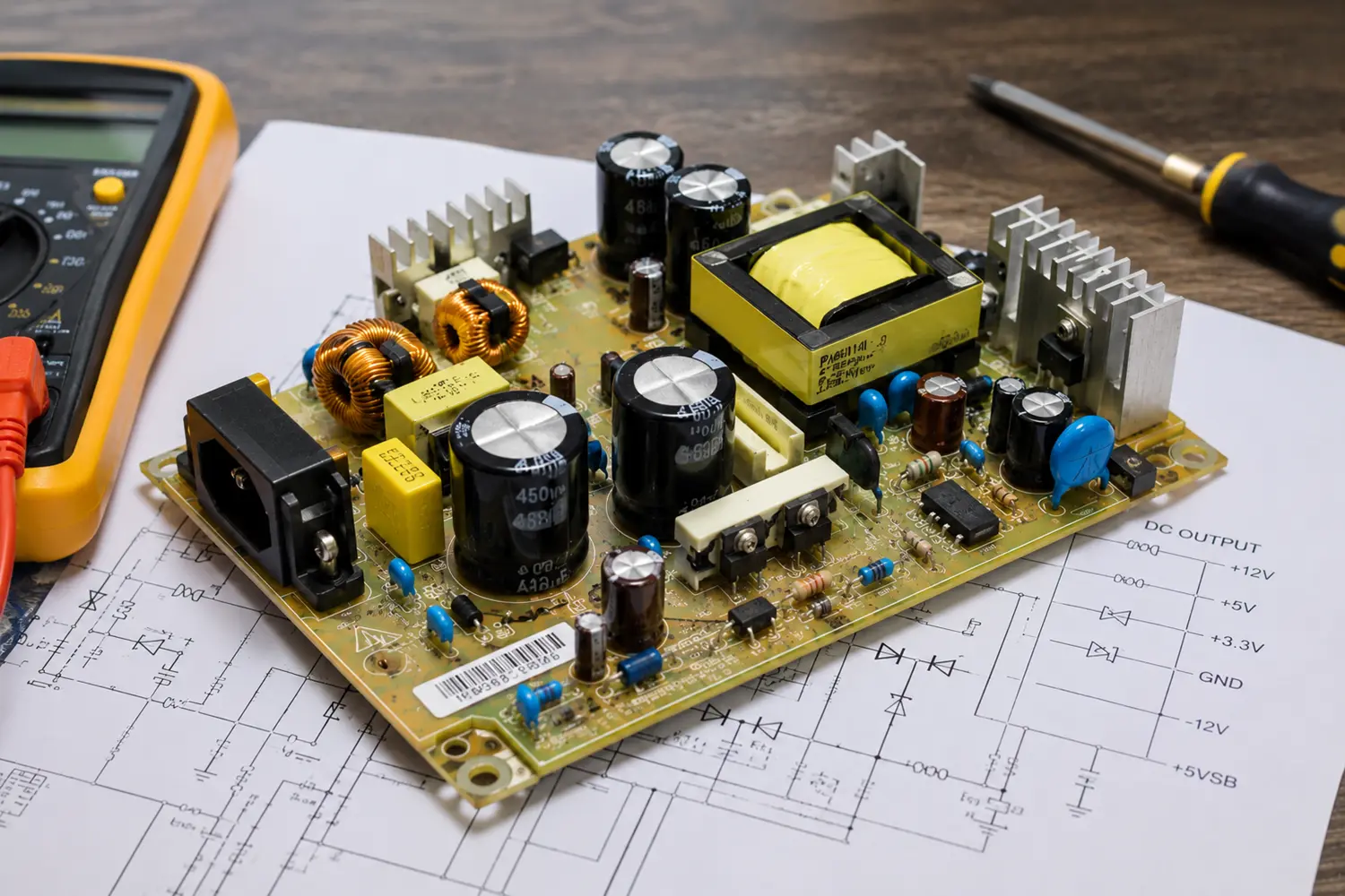
Every power supply circuit board, regardless of topology, is built around a set of fundamental components. Understanding each component's role, selection criteria, and failure modes is essential for reliable design.
2.1 Transformers
In AC-to-DC power supplies, the transformer is the first stage — stepping down high mains voltage (e.g., 230V AC) to a lower, safer AC voltage. In linear power supplies, a 50/60 Hz iron-core transformer is used. In switch-mode power supplies (SMPS), high-frequency ferrite-core transformers operate at tens to hundreds of kilohertz, enabling dramatic reductions in size and weight.
Key transformer selection parameters include: turns ratio (determining the voltage step-down), power rating (in VA or watts), isolation voltage (safety barrier between primary and secondary), and core material (laminated silicon steel for line-frequency, ferrite for high-frequency SMPS).
2.2 Rectifiers
The rectifier converts AC voltage into pulsating DC. The most common configurations are:
- Half-wave rectifier: Uses a single diode — simple but inefficient, with high ripple. Rarely used in quality designs.
- Full-wave bridge rectifier: Uses four diodes in a bridge configuration — the industry standard, providing full utilization of both AC half-cycles.
- Synchronous rectification: Uses MOSFETs instead of diodes in high-efficiency SMPS designs, dramatically reducing forward voltage drop losses.
2.3 Filter Capacitors
After rectification, the DC voltage still contains significant ripple. Filter capacitors (also called bulk capacitors or reservoir capacitors) smooth this ripple by storing charge during voltage peaks and releasing it during troughs. Electrolytic capacitors are typically used here due to their high capacitance-per-volume ratio. The capacitance value is calculated based on the load current, acceptable ripple voltage, and line frequency.
2.4 Voltage Regulators
The voltage regulator is the final precision stage that delivers a constant, stable output voltage despite variations in input voltage or load current. The two primary families are:
- Linear regulators (e.g., 7805, LM317, LDOs): Simple, low-noise, but inefficient — they dissipate excess voltage as heat.
- Switching regulators (buck, boost, buck-boost): Highly efficient (85-95%), but more complex and generate switching noise that requires careful filtering.
2.5 Protection Components
A well-designed power supply PCB includes multiple layers of protection: fuses and PTC resettable fuses for over-current protection, TVS diodes and MOVs (Metal Oxide Varistors) for transient voltage suppression, NTC thermistors for inrush current limiting, and crowbar circuits for over-voltage protection that can short the output to prevent damage to downstream electronics.
3. PCB Design & Layout Considerations
Even with perfect component selection, a poor PCB layout can render a power supply noisy, inefficient, or dangerously unreliable. Power supply PCB layout is a specialized discipline that differs significantly from low-speed digital or analog signal layout.
3.1 Trace Width & Copper Weight
Power supply traces carry significant current — often several amperes or more. Standard 1 oz/ft² copper may be insufficient. Use the IPC-2221 standard to calculate minimum trace widths for a given current and temperature rise. For high-current paths, consider 2 oz or 3 oz copper, or use solder-reinforced traces and bus bars. As a rule of thumb: for external traces on 1 oz copper, allow approximately 10 mils of width per ampere for a 10°C temperature rise.
3.2 Ground Plane & Star Grounding
Power supply grounding is critical for both performance and safety. Use a solid, unbroken ground plane on one or more layers. Implement star grounding — where all ground returns converge at a single point — to prevent high-current return paths from modulating sensitive reference grounds. Separate the power ground (high-current, noisy) from the signal ground (quiet, sensitive), and connect them at exactly one point, typically at the output capacitor's ground terminal.
3.3 Creepage & Clearance
For mains-connected power supplies, IPC-2221 and relevant safety standards (IEC 60950-1, IEC 62368-1) mandate minimum creepage (distance along a surface) and clearance (distance through air) between high-voltage and low-voltage sections. For 230V AC mains, typical minimum clearance is 2.5-4.0 mm depending on pollution degree and altitude. Use isolation slots (routed cutouts in the PCB) to increase creepage distance without consuming excessive board area.
3.4 Switching Node Layout
In SMPS designs, the switching node — where the power switch, diode, and inductor meet — has extremely high dV/dt. Minimize the copper area of this node to reduce radiated EMI. Keep the high-current AC loops (input capacitor → switch → inductor → output capacitor) as physically small as possible. A good rule: the entire high-frequency power loop should fit within a 1 cm × 1 cm area.
Common Layout Mistake
Never route sensitive feedback traces parallel to or near high dV/dt switching nodes. This capacitive coupling can inject noise into the feedback loop, causing instability, oscillation, and output voltage deviation. Keep feedback traces short, and consider using a ground guard trace or ground plane shielding.
4. Thermal Management Strategies
Power supplies generate heat — it's an unavoidable consequence of non-ideal components. Effective thermal management is the difference between a product that lasts 20 years and one that fails in months.
4.1 Identifying Hot Components
The primary heat sources in a power supply are: power semiconductors (MOSFETs, diodes, linear regulators), magnetics (transformers, inductors — due to core losses and copper I²R losses), and capacitors (especially electrolytics, whose ESR causes self-heating from ripple current). Use manufacturer-provided thermal resistance values (θJA, θJC) to estimate junction temperatures.
4.2 Copper Pour & Thermal Vias
Copper is an excellent thermal conductor. Use large copper pours connected to the thermal pad of power components. Thermal vias — small, densely packed plated-through holes under hot components — conduct heat to internal ground planes or the opposite side of the board. A 10×10 array of 0.3 mm vias can reduce thermal resistance by 50% or more compared to a bare pad.
4.3 Heatsinks & Active Cooling
For higher power levels, external heatsinks — extruded aluminum, stamped, or bonded-fin — are essential. Ensure proper thermal interface material (TIM) such as thermal paste, gap pads, or phase-change materials between the component and heatsink. When natural convection is insufficient, forced-air cooling with fans or blowers becomes necessary. Design the PCB layout to facilitate smooth airflow across hot components.
5. Critical Safety Considerations
Safety in power supply design is non-negotiable. A fault in the power supply can cascade into fire, electric shock, or destruction of expensive downstream equipment. Regulatory compliance — CE (Europe), UL (USA), BIS (India), CCC (China) — mandates rigorous safety design.
5.1 Mains Isolation
The isolation barrier between primary (mains) and secondary (user-accessible) sides is the single most important safety feature. This is achieved through the transformer (reinforced or double insulation), optocouplers for feedback, and Y-capacitors rated for line-to-ground applications (Y1 or Y2 safety class). The isolation must withstand a hipot test — typically 3000V AC for reinforced insulation — without breakdown.
5.2 Over-Current Protection (OCP)
Over-current conditions — from short circuits, component failures, or excessive load — can cause PCB trace fusing, component destruction, and fire. Implement multi-tier OCP: a primary fuse for catastrophic fault isolation, cycle-by-cycle current limiting in the SMPS controller, and hiccup-mode protection that periodically attempts restart rather than latching off permanently.
5.3 Over-Voltage Protection (OVP)
If the voltage regulation loop fails — for example, if the feedback resistor divider opens — the output voltage can rise to destructive levels. An independent OVP circuit monitors the output and triggers a crowbar (SCR that shorts the output) or shuts down the controller via a dedicated OVP pin. This is especially critical for supplies powering expensive FPGAs, ASICs, or processors.
5.4 Over-Temperature Protection (OTP)
NTC thermistors or silicon temperature sensors placed near hot components feed into a comparator or ADC input. When a threshold is exceeded, the controller reduces power, shuts down, or triggers a warning. This prevents thermal runaway — a dangerous positive-feedback cycle where increased temperature causes increased losses, which causes further temperature rise.
6. SMPS vs Linear Power Supply PCBs
The choice between switch-mode and linear power supply topologies is one of the first and most consequential decisions in a design. Each has distinct advantages and trade-offs.
| Parameter | Linear Power Supply | Switch-Mode Power Supply (SMPS) |
|---|---|---|
| Efficiency | 30-60% (poor) | 80-95% (excellent) |
| Output Noise | Very low (µV range) | Higher (mV range, switching ripple) |
| Size & Weight | Large, heavy (50/60 Hz transformer) | Compact, lightweight |
| Complexity | Simple, few components | Complex, requires careful EMI design |
| EMI | Minimal | Significant — requires filtering & shielding |
| Cost | Lower for low power | Lower for medium/high power |
| Best Applications | Audio, precision analog, sensitive RF | Most modern electronics, battery-powered, high-power |
In practice, many designs use a hybrid approach: an SMPS pre-regulator for efficient bulk voltage reduction, followed by a low-noise linear LDO for sensitive analog or RF rails. This combines the efficiency of SMPS with the noise performance of linear regulation.
7. Testing & Validation Protocols
No power supply design is complete without thorough testing. At AEAR, our testing protocol spans electrical performance, thermal behaviour, EMI compliance, and safety verification.
- Load regulation test: Measure output voltage deviation from 0% to 100% rated load. Target: less than ±1% for precision supplies.
- Line regulation test: Vary input voltage across its specified range and measure output variation. Critical for universal-input (90-264V AC) designs.
- Ripple & noise measurement: Using a 20 MHz bandwidth-limited oscilloscope probe with short ground spring — NOT the long ground clip lead.
- Efficiency measurement: Precision power meters on both input and output. Plot efficiency vs load curve across the operating range.
- Transient response: Apply a fast load step (e.g., 10% → 90% rated current) and observe output voltage deviation and recovery time.
- Thermal imaging: Run at full load in worst-case ambient temperature. Identify hotspots and verify all components stay within rated temperature limits.
- EMI pre-compliance scan: Using a spectrum analyzer and LISN (Line Impedance Stabilization Network) to identify potential conducted and radiated emissions issues before formal certification.
- Hipot & insulation resistance: Verify the isolation barrier integrity at 1.5× to 2× rated voltage plus 1000V, per applicable safety standard.
8. Conclusion & Best Practices
Designing a reliable, safe, and efficient power supply circuit board requires mastery of multiple disciplines — component engineering, PCB layout, thermal dynamics, magnetics design, control loop theory, and regulatory compliance. There are no shortcuts, and the cost of cutting corners in PSU design is measured in product returns, safety incidents, and brand reputation damage.
At AEAR, our PCB design team brings decades of combined experience in power electronics for defence, aerospace, industrial automation, and telecommunications applications. We design power supply boards that meet the most demanding standards — from MIL-STD for military applications to IPC Class 3 for high-reliability electronics.
AEAR Power Supply PCB Design Checklist
✓ Component derating (80% max for voltage, 70% max for power at worst-case temperature)
✓ Star grounding with single-point power/signal ground connection
✓ Adequate creepage/clearance per IEC 62368-1 for the target pollution degree
✓ Thermal simulation or measurement at max load, max ambient
✓ Independent OVP circuit separate from regulation feedback
✓ EMI filtering (common-mode choke, X and Y capacitors, ferrite beads)
✓ Fuse or PTC on every power input, sized for inrush and fault conditions
✓ Full test report documenting all measurements and pass/fail criteria
Rajesh Kumar
Excellent article! The section on creepage and clearance for mains-connected supplies was particularly helpful. We recently had a design fail hipot testing because of insufficient isolation slot depth — wish I'd read this first. Bookmarking for our next design review.
Sarah Peterson
Great deep dive into SMPS vs linear topologies. One thing I'd add: for ultra-low-noise analog designs, we've had success using an SMPS pre-regulator followed by an LDO with high PSRR at the switching frequency. Best of both worlds for efficiency and noise.
Michael Davidson
Your checklist at the end is gold — I've printed it out and stuck it on our lab wall. Especially appreciate the component derating recommendations. We've been running MOSFETs at 85% of rated Vds and it's bitten us more than once during hot-plug events.